
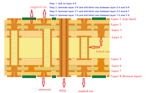
What Are the Primary Steps Involved in Stacked Microvias
Traditionally, conductive vias are created by drilling through a stack of circuit substrate layers and then plating the wall of the via with an electrically conductive material such as copper. The plated copper exerts high stress on the interface between the top and bottom substrate layers. This stress is exaggerated when multiple stacked vias are present. Failure modes can occur at the plated via/via and via/pad interfaces, or at the knee (where the copper slopes into the microvia at the via cap). Stacked microvias are also susceptible to stresses that arise from thermal cycling, including those caused by temperature variations during assembly.
In addition, the use of a variety of dielectric materials and via fabrication methods can have an impact on the reliability of stacked microvias. These factors can affect the proximity of a plated hole to the edge of the adjacent layer and the diameter of the plated hole. The type of laser used to drill the microvias, and the use of a photoimaging technology for etching and drilling may also affect the reliability of the via.
The failure rate of stacked microvias can be higher than that of staggered vias, depending on the design and manufacturing process. This is especially true when the stacked microvias are located close to a buried via hole, as this can cause stress at the metallurgical interface of the buried via hole and the bottom of the corresponding copper layer. The size of the voids within a microvia has also been found to have an effect on its failure rates. Smaller voids are more reliable, and larger voids have a greater risk of failing.
Stacked Microvias – What Are the Primary Steps Involved in Stacked Microvias?
It is also important to note that a plethora of variables can impact the reliability of a stacked microvia, including the selection of appropriate materials for laser drilling, adherence to IPC-T-50M guidelines and implementation of stack-up configurations in alignment with IPC-2226 standards. Additionally, the continuous monitoring of a microvia’s resistance during reflow can help to identify latent problems.
A number of PCB manufacturers have developed techniques for enhancing the reliability of stacked microvias, such as avoiding forming a via with a smaller diameter than the pad at its base, and using aluminum plate screen or hinder ink to plug the via after surface finish. This technology procedure can prevent solder connections from being formed in the via, and it is also a good practice to ensure that all of the vias on a printed circuit board are plugged after surface finish, as this will reduce potential signal integrity issues.
Sierra Circuits offers a wide range of standard and custom-designed PCBs with stacked and staggered vias. We can also provide a range of manufacturing services, including etching, drilling, plating and soldering to create a finished product that meets your specifications. To find out more, contact us today. Our team is happy to discuss your options for creating a cost-optimized PCB that incorporates staggered and stacked vias. You can also get started online with a free quote for your next project.