
PCB HDI technology offer
The development of new and improved PCB technology offers numerous advantages for manufacturers and consumers alike. One such benefit is the increased efficiency and performance of HDI (High-Density Interconnect) circuit boards. These types of boards offer increased functionality, a shorter timeframe for production and lower costs than traditional multilayer PCBs.
The design of these high-performance circuit boards requires careful planning and attention to detail to ensure that the final product performs as expected. pcb hdi are often used in complex electronic devices that demand excellent performance while conserving space. They are typically found in mobile / cellular phones, touch-screen devices, digital cameras, 4/5G network communications and even military applications such as smart munitions and avionics.
A main feature of these high-density circuit boards is their reduced dimensional footprint – a result of smaller pad sizes and fine pitch of the plated copper traces or pads on the board surface. In addition to their small size, these circuit boards also require higher precision than conservative PCB designs due to the miniature pads and fine pitch of the circuitry.
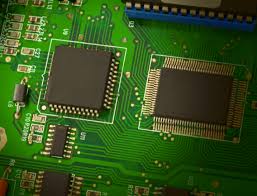
What cost-saving benefits does PCB HDI technology offer?
In order to achieve the required accuracy, a more complex manufacturing process is used for HDI boards. This process includes a pre-preg and copper layers that are fused together using heat and pressure during the lamination cycle. In addition, the metallization of the circuitry is performed in the via-in-pad method rather than through traditional via holes. This technique provides better quality metallization and reduces the risk of voids in the circuitry.
Another factor that contributes to the increased cost-efficiency of these high-performance boards is their reduced thickness. This translates to a reduction in the amount of raw materials needed and lowers production costs for both the manufacturer and the consumer. In addition, these smaller boards are able to accommodate more components on a single side, further decreasing production costs.
The use of HDI PCBs has been associated with decreased power consumption, resulting in a longer battery life for handheld devices. This is an important advantage, especially for products such as mobile / cellular phones that are frequently used and recharged. A longer battery life also decreases the amount of time that the device is on and decreases its energy expenditure, helping to save money and reduce environmental impact.
The production of an effective pcb hdi requires a high level of technical expertise and the latest state-of-the-art equipment for exacting precision. In addition, the selection of the appropriate components is critical to the successful implementation of any HDI project. The right choice will help to minimize costly delays, redesigns, or other production issues that may add to the overall cost of the project. Finally, it is important to consider the supplier’s ability to meet tight delivery schedules and provide fast turnaround times, as this can significantly reduce manufacturing costs for both the manufacturer and the customer.